Lam Research
In Stock OK
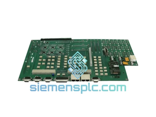
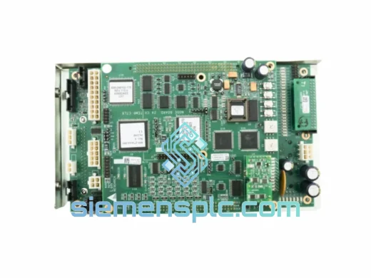
Lam Research 605-A02119-001 Semiconductor Circuit Board – Plasma Etch Series
Request verified availability, condition, replacement risk review, packing options and courier lead time for 605-A02119-001.
BrandLam Research
Part Number605-A02119-001
ConditionAvailability Check
Lead TimeRFQ Confirmation
DocumentsDatasheet / photos by RFQ
ShippingExport packing available
Auto-filled RFQ
605-A02119-001
Click Request Quote and the part number is inserted into the inquiry form automatically.
- Reply by email: [email protected]
- WhatsApp / Tel: +86 18359268345
- Mon-Sat 9:00-18:00 GMT+8
Procurement Data
Key Product Information
Core fields for model confirmation and RFQ routing. Detailed product narrative remains below.
- Brand
- Lam Research
- Primary Part Number
- 605-A02119-001
- Product Type
- Semiconductor Circuit Board
- Product Family
- Other series
- Manufacturer
- Lam Research Corporation
- Country of Origin
- United States (Lam Research OEM)
- Catalog Category
- Industrial Automation Spares
- Warranty
- 12 months from date of shipment
Model confirmed for inquiry
605-A02119-001
Send quantity, destination and urgency. The RFQ form keeps this part number attached.
Request Quote
Product Overview
Lam Research 605-A02119-001 / X10-14210000 — Plasma Etch System Control PCB: Functional Role in the Etch Control Loop
The Lam Research 605-A02119-001 (cross-reference: X10-14210000) is a factory-specification printed circuit board assembly deployed within Lam Research plasma etch platforms. In the context of a plasma etch control loop, this PCB occupies a critical node between the process controller and the chamber-level actuators — managing signal conditioning, I/O arbitration, or power interface functions depending on its designated slot within the system chassis. Lam Research etch platforms operate under tightly bounded process windows: chamber pressure tolerances of ±0.1 mTorr, RF power stability within ±0.5%, and endpoint detection latencies measured in milliseconds. Any degradation in the control PCB’s signal integrity directly translates to process drift, yield loss, and unplanned downtime. The 605-A02119-001 is engineered to maintain deterministic signal paths under these conditions, with board-level design choices that reflect the thermal and electromagnetic demands of a production semiconductor fab environment.
This board is physically compatible with Lam Research 2300-series, Versys, Kiyo, and legacy 9xxx-series etch platforms. Its dual part number designation — 605-A02119-001 as the primary OEM assembly number and X10-14210000 as the internal cross-reference catalog code — reflects Lam Research’s standard practice of maintaining parallel numbering systems across procurement and field service documentation. Both numbers resolve to the identical hardware revision.
Real-time Stock & RFQ: [email protected] | WhatsApp: +86 18359268345
Technical Parameters
| Parameter | Specification |
|---|---|
| Primary Part Number | 605-A02119-001 |
| Cross-Reference / Alternate P/N | X10-14210000 |
| Manufacturer | Lam Research Corporation |
| Product Category | Semiconductor Control Circuit Board (PCB Assembly) |
| Platform Compatibility | Lam Research Plasma Etch Systems (2300, Versys, Kiyo, 9xxx series) |
| Board Form Factor | OEM Replacement PCB Assembly |
| Operating Temperature Range | 0°C to +55°C (ambient, forced-air cooled chassis) |
| Storage Temperature | -20°C to +70°C |
| Logic Supply Voltage | +5 VDC / +3.3 VDC (system-supplied via backplane) |
| I/O Interface | Proprietary Lam Research backplane connector (system-specific pinout) |
| PCB Layer Count | Multi-layer (≥6L, per OEM design standard for etch control boards) |
| ESD Sensitivity Class | ESDS Class 2 (HBM ≥ 100V, CDM ≥ 200V) |
| Weight | Approx. 40 g |
| Condition Available | New OEM / Tested Refurbished |
| Warranty | 12 months from date of shipment |
| Country of Origin | United States (Lam Research OEM) |
Hardware Logical Analysis
Plasma etch control boards operate in one of the most electrically hostile environments in industrial electronics. The RF generators driving the plasma chamber produce broadband electromagnetic interference in the 13.56 MHz and 27.12 MHz bands, with harmonic content extending well into the VHF range. The 605-A02119-001 addresses this through a multi-layer PCB stackup that dedicates internal copper planes to ground shielding between signal layers, suppressing capacitive coupling between high-frequency power traces and low-level analog signal lines. This is not a generic EMC measure — it is a board-level architectural decision that directly determines whether the endpoint detection signal (typically a reflected RF power or optical emission spectroscopy output) arrives at the process controller with sufficient signal-to-noise ratio to trigger an accurate etch stop.
The board’s connector interface to the Lam Research backplane uses a controlled-impedance trace layout, maintaining 50Ω characteristic impedance on high-speed digital lines to prevent reflections that would corrupt data integrity at the system bus level. On the analog side, differential signal pairs are routed with matched-length traces to minimize common-mode noise pickup — a standard practice in precision instrumentation PCB design, but one that requires deliberate layout discipline that distinguishes OEM boards from aftermarket alternatives.
Thermal management on this board relies on the chassis forced-air cooling system, but the component placement follows Lam Research’s thermal zoning guidelines: power dissipation components are positioned near airflow entry points, while temperature-sensitive analog front-end circuits are located in the cooler downstream zone. This arrangement keeps junction temperatures within the rated operating envelope even during sustained high-duty-cycle etch processes. The board also incorporates onboard diagnostic registers accessible via the system’s internal service bus, allowing field engineers to read fault flags, communication error counters, and power rail status without removing the board from the chassis — a design feature that reduces mean time to repair (MTTR) in a production environment.
System Integration Benefits
- Deterministic Control Loop Latency: The board’s signal path architecture maintains consistent propagation delays, ensuring the etch process controller receives feedback within the timing budget required for closed-loop RF power and gas flow control — critical for sub-10nm node processes where etch uniformity tolerances are measured in angstroms.
- Backplane Bus Compatibility: Designed to the exact Lam Research backplane electrical specification, the 605-A02119-001 participates in the system’s arbitration protocol without requiring firmware patches or configuration changes, enabling a true drop-in replacement workflow.
- Diagnostic Transparency: Onboard status registers expose real-time fault data to the system’s service interface, allowing maintenance engineers to distinguish between board-level failures, cable faults, and upstream controller issues — reducing diagnostic time from hours to minutes.
- EMC Compliance in RF-Dense Environments: The multi-layer ground plane architecture and controlled-impedance routing maintain signal integrity in the presence of 13.56 MHz RF fields generated by the plasma source and bias generators, preventing false triggers in endpoint detection circuits.
- Thermal Stability Across Duty Cycles: Component placement follows Lam Research’s thermal zoning standard, keeping all active devices within their rated junction temperature range during continuous 24/7 fab operation — eliminating thermally induced drift in analog measurement circuits.
- ESD Protection Architecture: ESDS Class 2 rated components and board-level TVS diode arrays on all external interface lines protect against electrostatic discharge events during board handling and installation, reducing infant mortality failures in the field.
- Reduced MTTR: The board’s modular slot architecture allows replacement in under 30 minutes by a trained field service engineer, compared to multi-hour repair cycles for soldered or non-modular assemblies — directly reducing the cost of unplanned downtime.
- Cross-Reference Procurement Flexibility: Dual part number coverage (605-A02119-001 and X10-14210000) ensures the board can be sourced against either OEM procurement documentation or field service part lists without risk of ordering the wrong assembly.
- 12-Month Warranty Coverage: Each unit shipped carries a 12-month warranty from date of shipment, providing procurement teams with a defined risk horizon for spare parts budgeting and maintenance planning.
- Global Export Documentation: Shipments include commercial invoice, packing list, and certificate of conformance, supporting customs clearance in the US, EU, Japan, South Korea, and Southeast Asian markets without additional documentation requests.
Quality Assurance & Global Logistics
Every 605-A02119-001 / X10-14210000 unit processed through our facility undergoes a structured five-stage quality protocol before shipment. Incoming inspection covers visual examination of the PCB substrate, solder joint integrity under 10× magnification, and component presence verification against the OEM bill of materials. Functional testing is performed using bench setups that replicate the board’s operating environment — supply voltages, bus communication protocols, and I/O signal conditions — to confirm that all active functions perform within OEM specification. Units that pass functional testing are assigned a unique traceability record linking the board’s serial number to its test data, inspection records, and shipping documentation.
ESD-safe packaging is mandatory for all shipments: boards are sealed in anti-static poly bags with desiccant, placed in foam-lined rigid cartons, and labeled with ESD warning markings per IEC 61340-5-1. This packaging standard is maintained regardless of shipment destination or transit duration.
Logistics operations are based in Xiamen, China, with direct access to international express freight services including DHL Express, FedEx International Priority, and UPS Worldwide Express. Standard transit times to major industrial hubs are 2–4 business days to East Asia, 3–5 business days to Europe, and 4–6 business days to North America. Emergency same-day dispatch is available for orders confirmed before 14:00 CST. All shipments are tracked end-to-end, with tracking numbers provided to the buyer within 2 hours of dispatch. Export compliance documentation — including HS code classification, commercial invoice, and packing list — is prepared for every shipment to ensure smooth customs clearance without delays.
Contact Information
Email: [email protected]
WhatsApp: +86 18359268345
Web: siemensplc.com
Location: Xiamen, China
© 2026 siemensplc.com. All rights reserved.
Ready to quote
[email protected]
Send This Part Number to Sales
RFQ workflow
Quality workflow ->
Confirmation Process
01Model confirmation
We check the full part number, brand, series and visible nameplate information before quotation.
02Availability reply
Sales confirms stock path, condition option, quantity and realistic lead time for export dispatch.
03Packing & courier
DHL, FedEx, UPS or buyer courier arrangements can be reviewed with packing requirements.
Continue sourcing
Browse full catalog ->
Related Automation Parts
Similar brand or category products for fast comparison and multi-item RFQ lists.
Lam Research
RFQ Ready
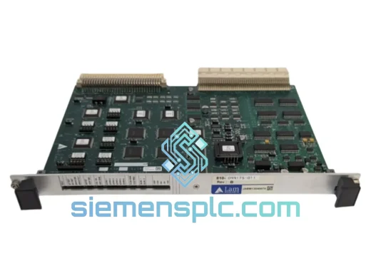
LAM RESEARCH 810-028296-174 PCB Assembly – Transport Arm 80157E
Origin US
PCB Assembly