TOKYO ELECTRON
RFQ Ready
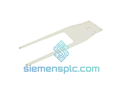
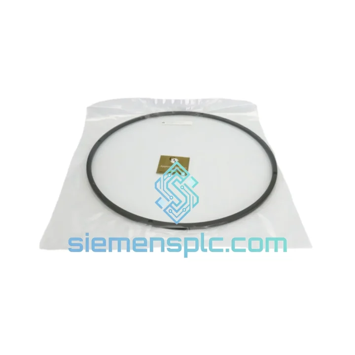
Tokyo Electron E2B023 ECU E2B023-11 ECUM Semiconductor Control Board – TEL ECU Series
Origin Japan
Semiconductor Equipment Control Board
Request verified availability, condition, replacement risk review, packing options and courier lead time for 1D10-203699-11.
Click Request Quote and the part number is inserted into the inquiry form automatically.
Core fields for model confirmation and RFQ routing. Detailed product narrative remains below.
The TOKYO ELECTRON 1D10-203699-11 is a precision-machined focus ring (also catalogued under alternate P/N 119151-01) engineered specifically for the PW3-32/900 plasma processing platform. Within a capacitively coupled plasma (CCP) etch chamber, the focus ring occupies the outermost annular position on the electrostatic chuck (ESC) assembly. Its primary function is to extend the plasma sheath uniformly across the wafer edge, preventing the characteristic roll-off of etch rate and ion flux that would otherwise degrade critical-dimension (CD) uniformity at the die periphery. Secondary functions include mechanical protection of the ESC dielectric surface and thermal boundary management at the wafer perimeter.
In the PW3-32/900 architecture, the focus ring interfaces directly with the lower electrode RF circuit. As the ring material erodes through ion bombardment over its qualified service life, the sheath geometry shifts progressively outward, causing measurable etch-rate non-uniformity (ERU) drift. TEL’s process qualification data for this platform specifies a replacement threshold based on cumulative RF hours and erosion depth, making part traceability and OEM dimensional conformance non-negotiable for yield-sensitive production environments.
Real-time Stock & RFQ: [email protected] | WhatsApp: +86 18359268345
| Parameter | Value / Specification |
|---|---|
| Manufacturer | TOKYO ELECTRON LIMITED (TEL) |
| Part Number | 1D10-203699-11 |
| Alternate / Cross-Reference P/N | 119151-01 |
| Compatible Platform | TEL PW3-32/900 CCP Etch / Deposition Chamber |
| Component Classification | Focus Ring (Edge Ring / Confinement Ring) |
| Substrate Material | High-purity silicon or quartz (confirm grade with TEL BOM) |
| Purity Grade | ≥ 99.999% (5N) for silicon variants; ≥ 99.99% for quartz variants |
| Wafer Size Compatibility | 200 mm / 300 mm (verify with chamber configuration) |
| Mounting Interface | Drop-in ESC peripheral seat — no hardware modification required |
| Surface Finish | Lapped / polished to OEM Ra specification |
| Approximate Weight | 1,450 g |
| Operating Temperature Range | −10 °C to +200 °C (chamber ambient) |
| RF Compatibility | 13.56 MHz primary; 2 MHz bias frequency (PW3-32/900 dual-frequency config) |
| Particle Specification | Cleaned to Class 10 / ISO 4 equivalent prior to packaging |
| Packaging | Double-bagged anti-static PE with desiccant; rigid outer carton |
| Country of Origin | Japan |
| Warranty | 12 months from date of shipment against manufacturing defects |
The 1D10-203699-11 focus ring operates within a dual-frequency RF excitation environment. The PW3-32/900 platform applies a high-frequency source power (13.56 MHz) to sustain plasma density and a low-frequency bias power (typically 2 MHz) to the lower electrode to control ion energy distribution function (IEDF). The focus ring, positioned concentrically around the wafer on the lower electrode, is electrically floating or weakly coupled depending on the chamber configuration. This floating potential allows the ring to self-bias under ion bombardment, which in turn shapes the local sheath potential at the wafer edge.
EMC and RF Shielding Geometry: The annular geometry of the 1D10-203699-11 is machined to tight concentricity tolerances (typically ±0.05 mm on inner diameter) to prevent asymmetric plasma perturbation. Any eccentricity in the ring seat introduces azimuthal non-uniformity in the RF sheath, which manifests as angular etch-rate variation across the wafer — a defect mode that is difficult to distinguish from process drift without detailed wafer mapping. The OEM dimensional specification eliminates this variable.
Erosion Mechanics and Replacement Logic: Under fluorine-based etch chemistries (e.g., CF₄/O₂, SF₆/C₄F₈), silicon focus rings erode at a rate proportional to ion flux density and bias power. TEL’s PM schedule for the PW3-32/900 defines a maximum erosion depth (typically 1.0–2.0 mm from the original top surface) beyond which sheath geometry deviation exceeds the process window. Quartz variants exhibit lower etch selectivity relative to silicon but offer superior thermal stability in high-power deposition processes. Material selection must align with the specific process chemistry and power regime in use.
Thermal Management at the Wafer Edge: The focus ring also functions as a thermal boundary element. In helium-backside-cooled ESC configurations, the ring’s thermal conductivity and contact geometry influence the radial temperature gradient at the wafer edge. Silicon rings (thermal conductivity ≈ 150 W/m·K) provide superior edge cooling compared to quartz (≈ 1.4 W/m·K), which is a critical consideration in thermally sensitive etch processes where photoresist selectivity is temperature-dependent.
Every TOKYO ELECTRON 1D10-203699-11 unit supplied through siemensplc.com is sourced from verified authorized distribution channels or factory-direct inventory. Pre-shipment inspection includes dimensional verification of inner diameter, outer diameter, and thickness against TEL OEM drawings; surface particle count inspection under cleanroom conditions; and visual examination for micro-cracks, chips, or surface contamination. A Certificate of Conformance (CoC) is available upon request for production-line quality records.
Logistics operations are managed from our warehouse in Xiamen, China. Standard international shipments are dispatched via DHL Express, FedEx International Priority, or UPS Worldwide Expedited, with typical transit times of 3–7 business days to major semiconductor manufacturing hubs in Taiwan, South Korea, the United States, Germany, and Singapore. For time-critical AOG (Aircraft on Ground equivalent) semiconductor line-down situations, same-day dispatch is available for in-stock units confirmed before 14:00 CST. All export documentation — including commercial invoice, packing list, and HS code classification — is prepared in compliance with Chinese customs regulations and destination-country import requirements.
Email: [email protected]
WhatsApp: +86 18359268345
Web: siemensplc.com
Location: Xiamen, China
© 2026 siemensplc.com. All rights reserved.
We check the full part number, brand, series and visible nameplate information before quotation.
Sales confirms stock path, condition option, quantity and realistic lead time for export dispatch.
DHL, FedEx, UPS or buyer courier arrangements can be reviewed with packing requirements.
Similar brand or category products for fast comparison and multi-item RFQ lists.