Mitsubishi Electric
RFQ Ready
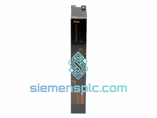
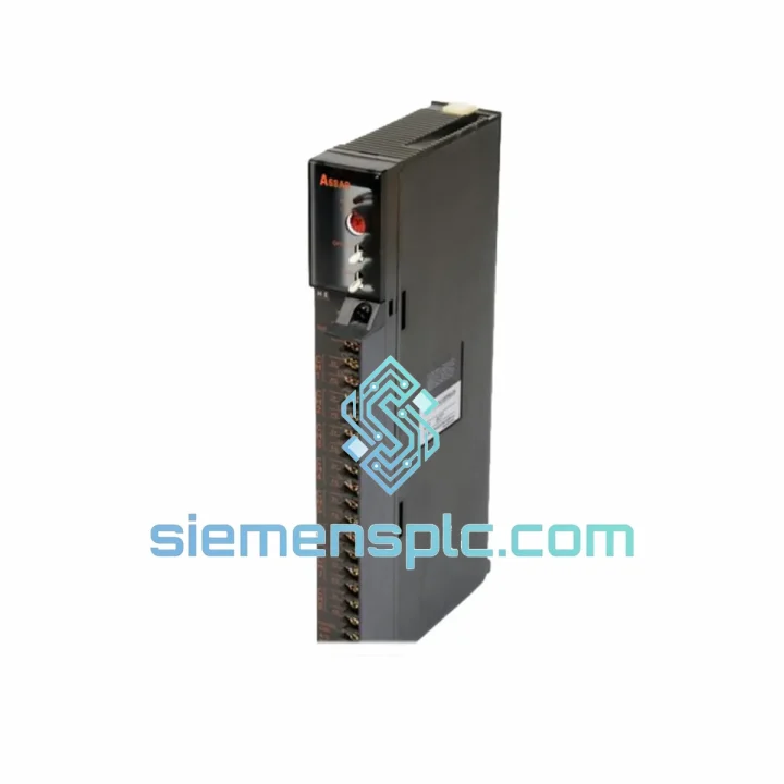
Mitsubishi Electric DOIOC11 DCS Digital Output Module
MELSEC-A
Origin JP
DCS Digital Output Module
Request verified availability, condition, replacement risk review, packing options and courier lead time for MELSEC-A.
Click Request Quote and the part number is inserted into the inquiry form automatically.
Core fields for model confirmation and RFQ routing. Detailed product narrative remains below.
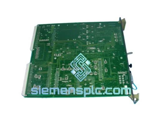
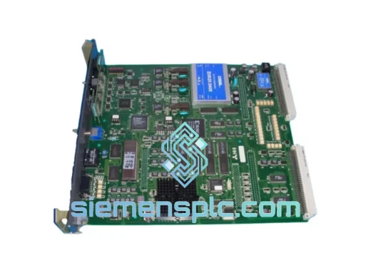
In any process control architecture built on the MELSEC-A platform, the analog input module occupies the most upstream position in the measurement chain. The A68AD fulfills this role by converting eight independent field-side analog signals — voltage or current — into 16-bit digital words that the CPU module reads each scan cycle via the A-Series parallel backplane bus. The module mounts directly on the main base or extension base as a local unit, requiring no dedicated communication interface card and no additional power supply beyond what the base unit provides. This local-unit architecture is the defining characteristic that separates the A68AD from remote I/O analog modules: data transfer is synchronous with the CPU scan, not asynchronous over a serial field bus, which means the CPU always reads a coherent, time-consistent snapshot of all eight process variables simultaneously.
The practical consequence of synchronous backplane transfer is measurable in PID loop behavior. When analog data arrives asynchronously — as it does in Profibus DP or CC-Link remote I/O configurations — the CPU must account for variable transport delay between the physical measurement event and the moment the data is available in the I/O buffer. This delay is not constant; it varies with bus load, token rotation time, and communication cycle jitter. In a tightly tuned PID loop with a fast process time constant, this jitter introduces phase error that degrades gain margin and can cause limit cycling. The A68AD eliminates this variable by placing the analog acquisition hardware on the same synchronous bus as the CPU, so the transport delay is fixed at one scan cycle — a deterministic, programmable quantity that the control engineer can account for precisely in loop tuning calculations.
Each of the eight channels accepts either a voltage input in the 0–10 V DC or ±10 V DC range, or a 4–20 mA current loop signal. Channel mode selection is performed via the module’s internal configuration registers, accessible through FROM/TO instructions in GX Developer or GX Works2. The input conditioning stage presents high impedance to voltage sources — typically greater than 1 MΩ — to avoid loading errors on transmitters with finite output impedance. For current inputs, a precision shunt resistor converts the loop current to a proportional voltage before the ADC stage. The shunt value is selected to produce a full-scale voltage that matches the ADC input range, maximizing the use of the converter’s dynamic range across the 4–20 mA span.
Analog-to-digital conversion uses a successive approximation register (SAR) architecture. The SAR method performs conversion by iteratively comparing the input voltage against a binary-weighted DAC reference, resolving one bit per clock cycle from the most significant bit downward. For a 16-bit converter, this requires 16 comparison cycles plus settling time, producing a conversion time that is short relative to the process time constants of most industrial measurements — temperature, pressure, flow, and level — while providing resolution sufficient to represent the full input range in increments of approximately 0.015% of full scale. The SAR architecture also exhibits well-characterized linearity behavior: integral nonlinearity (INL) and differential nonlinearity (DNL) errors are bounded and stable over the operating temperature range, unlike sigma-delta converters whose noise-shaping behavior can produce artifacts in the presence of low-frequency input signals.
Optical isolation is implemented between the field-side signal conditioning and ADC circuitry and the backplane-side digital interface logic. The isolation barrier is placed after the ADC — the analog-to-digital conversion occurs on the field-side circuit, and the resulting digital word is transferred across the optical barrier as a serial digital signal. This post-ADC isolation topology avoids the accuracy limitations of analog optocoupler designs, where the LED-photodetector transfer characteristic introduces nonlinearity and temperature-dependent gain variation. By isolating the digital output of the ADC rather than the analog input, the A68AD preserves the full linearity specification of the SAR converter across the isolation boundary. The isolation barrier is rated to withstand surge transients per IEC 61000-4-5, protecting the CPU and backplane from ground loop currents and switching transients that propagate through field wiring in installations with distributed grounding or adjacent high-power switching equipment.
For maintenance engineers managing legacy MELSEC-A installations, the A68AD’s hardware interface is fully defined by the published A-Series hardware specification. The module’s slot address, I/O buffer memory map, and FROM/TO instruction interface are identical across production batches, enabling direct replacement without modification to existing ladder logic programs, CPU parameter files, or base unit wiring. This drop-in compatibility is a quantifiable advantage in maintenance scenarios: the mean time to repair is bounded by the physical replacement procedure rather than by software reconfiguration or recommissioning activities.
Real-time Stock & RFQ: [email protected] | WhatsApp: +86 18359268345
| Parameter | Specification |
|---|---|
| Model Number | A68AD |
| Manufacturer | Mitsubishi Electric Corporation |
| Series | MELSEC-A Series |
| Module Type | Analog Input Local Unit |
| Number of Input Channels | 8 (independently configurable) |
| Voltage Input Range | 0–10 V DC / ±10 V DC (per channel) |
| Current Input Range | 4–20 mA DC (per channel) |
| A/D Conversion Method | Successive Approximation Register (SAR) |
| Output Resolution | 16-bit digital word per channel |
| Isolation Architecture | Post-ADC optical isolation, field-side to backplane-side |
| Backplane Interface | MELSEC-A Series synchronous parallel backplane bus (local unit) |
| Compatible CPU Modules | A2UCPU, A3UCPU, A1SCPU, A2SCPU, A2ACPU and compatible A-Series CPUs |
| Compatible Base Units | A38B, A35B, A32B main base; A-Series extension bases |
| Programming Interface | FROM/TO instructions via GX Developer / GX Works2 |
| Operating Temperature | 0 to 55 °C |
| Storage Temperature | −25 to 75 °C |
| Module Weight | Approx. 1,210 g |
| Country of Origin | Japan |
| Warranty | 12 months from shipment date |
The A68AD’s internal signal path begins at the screw-terminal input block, where field wiring connects to the per-channel conditioning stage. The conditioning stage performs three functions before the signal reaches the ADC: impedance transformation, range scaling, and anti-aliasing filtering. For voltage inputs, the high-impedance buffer stage prevents the module from loading the transmitter output, which is critical when the transmitter has a finite output impedance or when multiple loads share the same signal source. For current inputs, the precision shunt resistor — selected for low temperature coefficient to minimize gain drift over the operating temperature range — converts the 4–20 mA loop current to a voltage proportional to the ADC input range.
The anti-aliasing filter is a passive RC low-pass network with a cutoff frequency set well below the ADC sampling rate. Its function is to attenuate signal components above the Nyquist frequency before digitization, preventing aliasing artifacts from appearing in the conversion output. For process measurement applications — where the physical variable of interest changes slowly relative to the ADC sampling rate — the primary benefit of this filter is noise rejection: it attenuates broadband electrical noise that couples into the signal cable from adjacent power wiring, variable frequency drives, and switching power supplies in the control panel.
The PCB layout separates the analog signal traces from the digital logic domain using a split ground plane topology. The analog ground plane underlies the input conditioning and ADC circuitry; the digital ground plane underlies the backplane interface logic. The two planes connect at a single point near the ADC’s digital output, minimizing the return current path for digital switching noise through the analog ground. This layout practice reduces the digital noise floor seen by the ADC, which directly affects the effective number of bits (ENOB) the converter achieves in the installed environment — a parameter that is more meaningful than the nominal 16-bit resolution when the module is operating in an electrically noisy industrial panel.
The module housing provides mechanical shielding against radiated electromagnetic fields from adjacent equipment. The metal enclosure acts as a Faraday cage for frequencies above the shield’s cutoff, attenuating electric field coupling from high-frequency sources such as servo drive PWM switching harmonics and radio-frequency interference from wireless devices in the plant environment. Combined with the optical isolation barrier and the PCB-level EMC layout, this three-layer shielding approach — housing, PCB layout, and galvanic isolation — addresses the three primary EMC coupling mechanisms: radiated field coupling, conducted common-mode interference, and ground loop currents.
Every A68AD unit supplied through siemensplc.com is sourced as genuine Mitsubishi Electric hardware through documented procurement channels with full unit traceability. Pre-shipment inspection covers physical condition assessment — PCB integrity, terminal block condition, housing label verification, and connector pin inspection — followed by packaging in anti-static bags with shock-absorbing foam inserts inside double-wall corrugated cartons. This packaging specification is designed to protect the module’s analog input circuitry, which is sensitive to electrostatic discharge and mechanical shock during transit.
All shipments originate from Xiamen, China, with access to DHL Express, FedEx International Priority, and UPS Worldwide Expedited services. Typical transit times are 3–5 business days to Southeast Asia, 5–7 business days to Europe and the Middle East, and 5–8 business days to North America, subject to customs clearance at the destination port. Each shipment includes a commercial invoice, packing list, and certificate of origin documentation prepared for customs declaration of industrial electronic components. A 12-month warranty from the shipment date covers confirmed manufacturing defects and hardware failures under normal operating conditions as defined in the Mitsubishi Electric A68AD hardware manual.
Email: [email protected]
WhatsApp: +86 18359268345
Web: siemensplc.com
Location: Xiamen, China
© 2026 siemensplc.com. All rights reserved.
We check the full part number, brand, series and visible nameplate information before quotation.
Sales confirms stock path, condition option, quantity and realistic lead time for export dispatch.
DHL, FedEx, UPS or buyer courier arrangements can be reviewed with packing requirements.
Similar brand or category products for fast comparison and multi-item RFQ lists.